
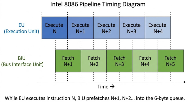
When Intel designed the 8086 in 1978, they made one decision that separated it from every processor before it: split the chip in two. One half fetches the next instruction while the other is still executing the current one. That single idea — two units working in parallel — created the foundation of every x86 pipeline that followed, right through to today’s Core processors. But before those two internal units can do anything, the chip has to talk to the outside world through exactly 40 pins. Understanding how those pins are assigned, multiplexed, and controlled is just as important as understanding what happens inside.
The 8086 divides itself into the Bus Interface Unit (BIU) — which owns the external address and data buses, the segment registers, the instruction pointer, and the prefetch queue — and the Execution Unit (EU) — which owns the ALU, general-purpose registers, and the flag register. The EU cannot touch the external bus. Every byte that moves between the CPU and memory or I/O goes through the BIU. The EU talks to the BIU through an internal 16-bit bus, requesting memory reads/writes and feeding back branch targets when jumps occur.
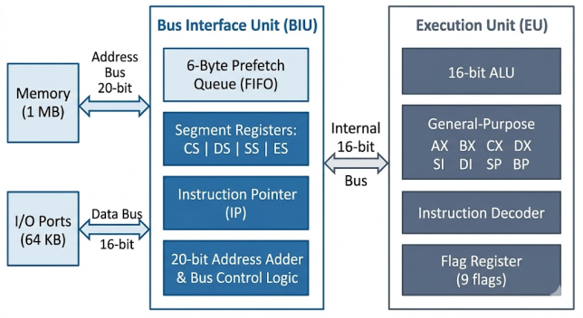
Segment Registers
The BIU contains four 16-bit segment registers. Each one defines the base of a 64 KB window into the 1 MB address space.
| Register | Name | Role |
|---|---|---|
| CS | Code Segment | Points to the segment containing the currently executing code. The IP register always offsets from CS. |
| DS | Data Segment | Default segment for nearly all data-access instructions. |
| SS | Stack Segment | Base of the stack. Every PUSH, POP, CALL, and RET uses SS:SP automatically. |
| ES | Extra Segment | Destination segment for all string instructions. The destination address is always ES:DI. |
Physical Address Generation: Segment:Offset
The segment register is shifted left by 4 bits (×16), then the 16-bit offset is added. The result is a unique 20-bit address.
General-Purpose Registers
| Register | Name | 8-bit Halves | Primary Role |
|---|---|---|---|
| AX | Accumulator | AH / AL | Holds results of arithmetic; required by MUL, DIV, IN, OUT |
| BX | Base | BH / BL | Memory base address — the only data register usable as a pointer in indirect addressing |
| CX | Counter | CH / CL | Loop counter for LOOP/LOOPZ/LOOPNZ; CL holds the shift/rotate count; REP prefix decrements CX |
| DX | Data | DH / DL | I/O port address with indirect IN/OUT; holds the high 16-bit word in 32-bit MUL and DIV (DX:AX pair) |
| SI | Source Index | — | Source pointer for string instructions (DS:SI) |
| DI | Destination Index | — | Destination pointer for string instructions (ES:DI) |
| SP | Stack Pointer | — | Always points to the top of the stack (SS:SP) |
| BP | Base Pointer | — | Stack frame base address; [BP+offset] accesses function parameters through SS |
The 6-Byte Prefetch Queue
Every taken branch (JMP, CALL, RET, taken Jcc, LOOP, INT) flushes all 6 bytes from the prefetch queue. The BIU then needs ~3 bus cycles to refill. This is why tight loops with many branches can be slower than equivalent straight-line code.
The BIU keeps a 6-byte FIFO buffer of upcoming instruction bytes, filling it from memory two bytes at a time whenever the bus is free. The EU pulls bytes from the front of this queue as it decodes and executes instructions. Three rules govern the queue: the BIU fills it whenever at least 2 bytes are empty and the EU hasn’t requested the bus for data; it pauses filling when the EU needs a memory or I/O access; and it flushes completely on any branch.
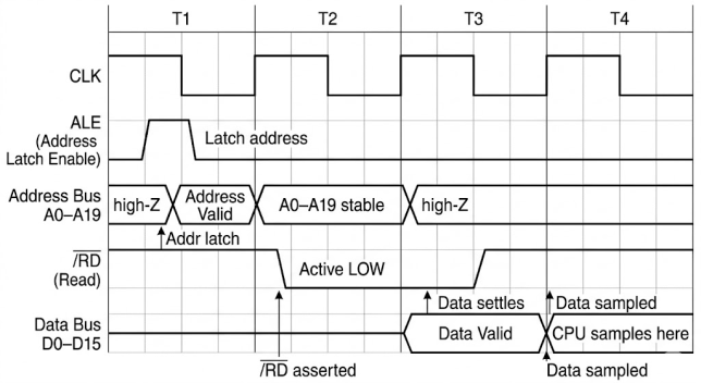
T-States and Bus Cycle Timing
| T-State | What Happens | Duration @ 5 MHz |
|---|---|---|
| T1 | BIU drives address bus; ALE pulses high | 200 ns |
| T2 | RD/WR strobed; address floated for data | 200 ns |
| T3 | READY sampled; data on bus | 200 ns |
| Tw | Wait state — inserted if READY=LOW (slow memory) | 200 ns each |
| T4 | Data latched by CPU or written to memory | 200 ns |
Minimum bus cycle: 4 T-states = 800 ns @ 5 MHz. Each Tw adds 200 ns.
Pin Diagram & Signal Reference
The 8086 is housed in a 40-pin DIP (Dual In-line Package). Fitting a 20-bit address bus, a 16-bit data bus, and all control signals into 40 pins required one key trick: address/data multiplexing. Pins AD0–AD15 carry the 20-bit address during T1, then switch to carry the 16-bit data word during T2–T4. The ALE signal tells external latch chips (typically the Intel 8282) when to capture and hold the address so it remains valid while the pins switch to data mode. A16–A19 are not multiplexed — they carry the upper 4 address bits throughout the entire bus cycle.
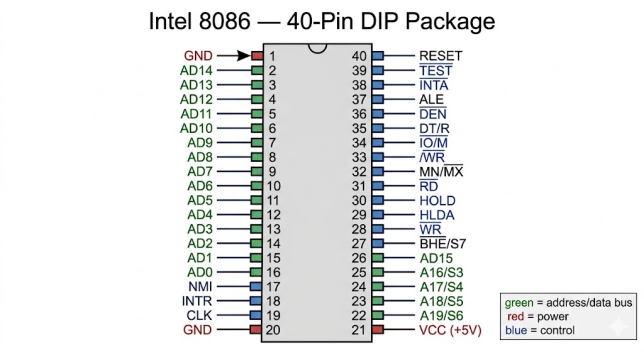
Complete 40-Pin Signal Table
| Pin(s) | Signal | Dir | Function |
|---|---|---|---|
| ADDRESS / DATA BUS (multiplexed) | |||
| 2–16, 26 | AD0–AD15 | I/O | Multiplexed address (A0–A15 during T1 while ALE is HIGH) and data (D0–D15 during T2–T4). External 8282 latches capture the address on the falling edge of ALE. |
| 22–25 | A16/S3–A19/S6 | O | Upper 4 address bits (A16–A19) during T1; segment status (S3–S6) during T2–T4. S3/S4 encode which segment register was used; S5 = IF; S6 = 0 always. |
| 27 | BHE/S7 | O | Bus High Enable (active LOW) during T1: selects the odd memory bank (D8–D15). LOW = odd bank active. S7 during T2–T4 (undefined, always HIGH). |
| CONTROL SIGNALS (both modes) | |||
| 37 | ALE | O | Address Latch Enable. HIGH during T1 to signal that AD0–AD15 carry a valid address. External 8282 latches latch the address on the falling edge. Never floated or three-stated. |
| 31 | /RD | O | Read strobe (active LOW). Asserted during T2–T4 of a memory or I/O read cycle. Memory or peripheral places data on the bus while /RD is LOW. |
| 19 | CLK | I | System clock input. All internal timing is derived from CLK. Requires 33% duty cycle. 5 MHz on original 8086; 8 MHz on 8086-2; 10 MHz on 8086-4. |
| 40 | RESET | I | Active HIGH. Must be held HIGH for at least 4 CLK cycles. On release, CPU sets CS=FFFFh, IP=0000h (reset vector FFFF0h) and begins execution. All flags and segment registers except CS are cleared. |
| 17 | NMI | I | Non-Maskable Interrupt. Rising edge triggers INT 2, regardless of IF flag. Cannot be blocked by CLI. Used for RAM parity errors and catastrophic hardware faults. |
| 18 | INTR | I | Maskable interrupt request. Sampled at the end of each instruction. Acknowledged only if IF=1 (STI). The 8259 PIC drives this line and supplies the vector number during /INTA. |
| 39 | /TEST | I | WAIT instruction samples this pin. If /TEST is HIGH, the CPU idles (inserts wait states) until /TEST goes LOW. Used to synchronize with the 8087 FPU — the 8087 drives BUSY to /TEST. |
| 32 | MN//MX | I | Mode select. Tie HIGH (to VCC) for Minimum Mode; tie LOW (to GND) for Maximum Mode. This single pin changes the function of eight control pins (28–31, 33–36). |
| MINIMUM MODE ONLY (MN//MX = HIGH, pins 28–31, 33–36) | |||
| 28 | /WR | O | Write strobe (active LOW). Asserted during a memory or I/O write cycle. Memory/peripheral latches data from AD0–AD15 on the rising edge of /WR. |
| 29 | HLDA | O | Hold Acknowledge. CPU floats AD0–AD15, A16–A19, BHE, /RD, /WR, DEN and asserts HLDA to confirm that a DMA controller may use the bus. |
| 30 | HOLD | I | Bus hold request from a DMA controller or bus master. CPU finishes the current bus cycle, floats the bus, and asserts HLDA. Bus is surrendered until HOLD goes LOW. |
| 33 | M//IO | O | Memory / I/O select. HIGH = memory access; LOW = I/O port access. External decode logic uses this to route the bus to memory chips or I/O peripherals. |
| 34 | DT//R | O | Data Transmit/Receive. Controls the direction of 8286 data bus transceivers. HIGH = transmit (CPU writing); LOW = receive (CPU reading). |
| 35 | /DEN | O | Data Enable (active LOW). Enables 8286 bus transceivers. Asserted during T2–T4 of any data transfer cycle. Kept HIGH (disabled) during address phase and idle. |
| 36 | /INTA | O | Interrupt Acknowledge (active LOW). Two consecutive /INTA pulses are generated when a hardware interrupt is accepted. The 8259 PIC places the 8-bit vector number on the data bus during the second pulse. |
| MAXIMUM MODE ONLY (MN//MX = LOW, pins 28–31, 33–36) | |||
| 28 | /S0 | O | Bus cycle status bit 0. Combined with S1 and S2, the 8288 Bus Controller decodes these to generate /MRDC, /MWTC, /IORC, /IOWC, /INTA command signals for the system bus. |
| 29 | /S1 | O | Bus cycle status bit 1. See S0 above. |
| 30 | /S2 | O | Bus cycle status bit 2. S2/S1/S0 = 000: /INTA; 001: I/O read; 010: I/O write; 011: halt; 100: code fetch; 101: memory read; 110: memory write; 111: passive (no bus cycle). |
| 31 | /LOCK | O | Bus Lock (active LOW). Asserted during LOCK-prefixed instructions. Prevents other bus masters (DMA) from taking the bus mid-sequence — essential for atomic read-modify-write operations. |
| 33 | /RQ//GT0 | I/O | Request/Grant 0 (active LOW, bidirectional). Replaces HOLD/HLDA in max mode. A pulse from an external master requests the bus; the CPU responds with a grant pulse; a third pulse signals the master is done. Higher priority than RQ//GT1. |
| 34 | /RQ//GT1 | I/O | Request/Grant 1 (active LOW, bidirectional). Same protocol as RQ//GT0 but lower priority. Allows two separate bus masters (e.g., 8089 IOP and 8087 FPU) to share the bus. |
| 35 | QS0 | O | Queue Status bit 0. Combined with QS1, tells the 8087 FPU what the 8086 prefetch queue just did so the 8087 can track the instruction stream. See table below. |
| 36 | QS1 | O | Queue Status bit 1. QS1/QS0: 00 = no operation; 01 = first byte of opcode from queue; 10 = queue flushed; 11 = subsequent byte of instruction. |
| POWER | |||
| 1, 20 | GND | — | Ground (0 V). Two separate GND pins for current return; both must be connected. |
| 21 | VCC | — | +5 V supply. Maximum 360 mA at 5 MHz. Decouple with 100 nF ceramic capacitor close to pin 21. |
Minimum Mode vs Maximum Mode
The MN//MX pin (pin 32) is the most unusual feature of the 8086 package: a single input that reconfigures eight output pins and changes the fundamental bus control architecture. You tie it permanently at board design time — it is not a runtime switch.
| Aspect | Minimum Mode (MN//MX = HIGH) | Maximum Mode (MN//MX = LOW) |
|---|---|---|
| Bus control generated by | 8086 directly (/WR, M//IO, DT//R, /DEN, /INTA) | External 8288 Bus Controller (decodes S0–S2) |
| Bus arbitration | HOLD / HLDA (simple request/grant) | /RQ//GT0, /RQ//GT1 (pulse protocol, two masters) |
| Coprocessor support | Not designed for 8087 (no QS0/QS1 queue status) | Full 8087 FPU support via QS0/QS1 and /RQ//GT |
| Multiprocessor support | Single master only | Up to 2 additional bus masters (8089 IOP, 8087 FPU) |
| Typical use | Simple single-board systems, educational kits | IBM PC, multiprocessor systems, systems with 8087 |
| Additional chip required | None (CPU drives bus directly) | Intel 8288 Bus Controller (mandatory) |
A 20-bit address bus + 16-bit data bus + control signals would need at least 56 pins if all were dedicated. Intel compressed this to 40 pins by sharing AD0–AD15 between address and data duties, switching roles each bus cycle under ALE timing. The external 8282 address latch (or 74LS373) holds the address stable while those pins carry data, so the memory subsystem sees a clean non-multiplexed interface. This trade-off added one clock cycle of latency per bus transaction but kept the chip in the inexpensive 40-pin DIP package.
Instruction Timing: Clock Cycles per Instruction
The T-state table above describes a single bus cycle. Most instructions require several bus cycles plus internal EU processing time on top. Total instruction time is calculated as:
EA clocks are added when the instruction uses a memory addressing mode. Each memory read or write costs a further 4 T-states minimum.
| Instruction | Form | Clocks | Notes |
|---|---|---|---|
| DATA TRANSFER | |||
| MOV | reg ← reg | 2 | Fastest data move |
| MOV | reg ← immediate | 4 | |
| MOV | reg ← memory | 8+EA | Add EA clocks from addressing mode |
| PUSH reg | SP−=2, write | 15 | Includes bus write cycle |
| POP reg | read, SP+=2 | 12 | Includes bus read cycle |
| ARITHMETIC | |||
| ADD / SUB | reg, reg | 3 | Sets CF, ZF, SF, OF, PF, AF |
| MUL | 16-bit | 118–133 | Most expensive common instruction |
| DIV | 16-bit | 144–162 | Use SHR for power-of-2 division |
| CONTROL FLOW | |||
| Jcc | taken | 16 | Flushes queue; refill penalty |
| Jcc | not taken | 4 | No flush; queue remains valid |
| CALL near | push IP, jump | 19 | Stack write + queue flush |
| INT n | software interrupt | 51 | Push FLAGS+CS+IP, IVT lookup, jump |
| STRING (per iteration with REP) | |||
| MOVSB / MOVSW | REP | 17 | MOVSW copies 2 bytes in same 17 clocks |
| STOSB / STOSW | REP | 11 | Fastest buffer fill; prefer STOSW |
EA clock costs: [BX]/[SI]/[DI] = 5 • [BX+SI]/[BP+DI] = 7 • [BX+DI]/[BP+SI] = 8 • [BX+disp] = 9 • Segment override adds 2.
Flag Register
The EU maintains a 16-bit flag register. Nine of its bits are active — six are status flags that reflect the outcome of the last arithmetic or logic instruction, and three are control flags that alter how certain instructions behave. Every conditional jump (Jcc) and conditional repeat (REP) tests one or more of these flags before deciding whether to act. The full flag reference is covered in the Flag Register post.
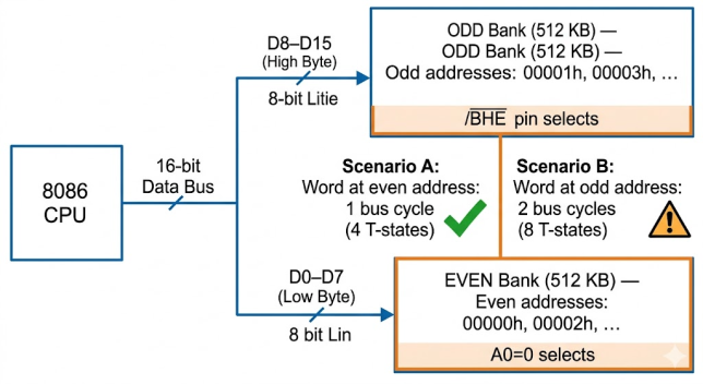
Even and Odd Memory Banks
Always place word variables at even addresses. A word (DW) at an even address transfers in 1 bus cycle (800 ns). The same word at an odd address requires 2 bus cycles (1,600 ns) — a 100% penalty the CPU handles silently. /BHE selects the odd bank; A0 selects the even bank.
The 8086 has a 16-bit external data bus, so the 1 MB address space is split into two interleaved 512 KB banks. The even bank (even addresses) connects to D0–D7, selected by A0=0. The odd bank (odd addresses) connects to D8–D15, selected by /BHE=0 (pin 27). A word read at an even address hits both banks in one bus cycle. A word read at an odd address requires two bus cycles because the bytes span a bank boundary.
The I/O Subsystem
The 8086 supports a separate 64 KB I/O port space accessed exclusively with IN and OUT instructions. The M//IO pin (pin 33 in minimum mode) distinguishes port access (LOW) from memory access (HIGH), allowing external decoding logic to route the bus to the correct chip.
; Direct port addressing (ports 00h-FFh only)
IN  AL, 60h         ; read keyboard port
OUT 61h, AL         ; write speaker/system control

; Indirect addressing via DX (ports 0000h-FFFFh)
MOV DX, 0378h       ; LPT1 data register
OUT DX, AL          ; write to parallel port
8255A PPI — Parallel I/O
The 8255A provides 24 configurable I/O lines in three 8-bit ports (A, B, C). A control byte written to the control register configures each port as input or output.
MOV DX, 0063h       ; 8255 control register
MOV AL, 82h         ; A=output, B=input, C=output
OUT DX, AL

MOV DX, 0060h       ; Port A
MOV AL, 0FFh
OUT DX, AL          ; drive all Port A lines HIGH

MOV DX, 0061h       ; Port B
IN  AL, DX          ; read 8 input lines into AL
8259A PIC — Interrupt Controller
The 8259A manages hardware interrupt lines IRQ0–IRQ7 and tells the CPU which vector number to load from the IVT. The IBM PC maps IRQ0–IRQ7 to INT 08h–0Fh.
; Initialize 8259A (IBM PC standard)
MOV AL, 13h         ; ICW1: edge-triggered, cascade, ICW4 needed
OUT 20h, AL
MOV AL, 08h         ; ICW2: base vector 08h
OUT 21h, AL
MOV AL, 00h         ; ICW3: no slave
OUT 21h, AL
MOV AL, 01h         ; ICW4: 8086 mode
OUT 21h, AL

; End-of-Interrupt (send at end of every hardware ISR)
MOV AL, 20h
OUT 20h, AL
8253 Timer — Programmable Interval Timer
The 8253 provides three 16-bit countdown timers clocked at 1.193182 MHz in the IBM PC. Channel 0 drives IRQ0 (18.2 Hz system tick). Channel 2 drives the PC speaker.
; Reprogram Channel 0 for 1 kHz timer ticks (divisor = 1193)
MOV AL, 36h         ; Ch0, LSB+MSB, Mode3, binary
OUT 43h, AL
MOV AX, 1193
OUT 40h, AL
MOV AL, AH
OUT 40h, AL

; Generate 440 Hz tone on PC speaker
MOV AL, 0B6h
OUT 43h, AL
MOV AX, 2712        ; 1193182 / 440 = 2712
OUT 42h, AL
MOV AL, AH
OUT 42h, AL
IN  AL, 61h
OR  AL, 03h
OUT 61h, AL         ; enable speaker
8086 vs 8088
| Feature | 8086 | 8088 |
|---|---|---|
| External data bus | 16-bit | 8-bit |
| Prefetch queue | 6 bytes | 4 bytes |
| Word at even address | 1 bus cycle | 2 bus cycles |
| /BHE pin | Present (pin 27) | Not present (SS0 instead) |
| IBM PC use | XT clones, AT era | Original IBM PC 5150 (1981) |
Read Next & Related Articles
- Read next: ⑤ Addressing Modes — EA calculation and string instructions that the EU processes
- ⑥ Flag Register — all 9 flags that the EU’s ALU sets
- ⑦ Stack Operations — SS:SP stack mechanics with PUSH/POP/CALL/RET
- ⑧ Interrupt System — the /INTA bus cycle sequence and 8259 initialization in full depth
- ① Introduction & Memory Segmentation — the 20-bit address formula and 8086 history
FAQs
Q: Why is the prefetch queue 6 bytes?
Six bytes is enough to buffer three 2-byte fetch cycles — enough to hide one round of fetch latency while the EU executes. The 8088’s 4-byte queue provides the same effect relative to its narrower 8-bit bus.
Q: What is the 8086 reset vector?
On RESET, CS=FFFFh and IP=0000h, so execution starts at physical address FFFF0h — the top 16 bytes of the 1 MB space, where ROM BIOS places a far jump to initialization code.
Q: What does /INTA do?
When a hardware interrupt is acknowledged, the BIU performs two consecutive /INTA bus cycles. During the second cycle the 8259 places the 8-bit interrupt vector number on the data bus; the CPU reads it, multiplies by 4, and loads CS:IP from the IVT.
Q: When would you use Maximum Mode?
Any time you add an 8087 FPU or a second bus master (like the 8089 IOP) to the system. Maximum mode’s QS0/QS1 pins let the 8087 shadow the 8086’s instruction queue so it can identify ESC (floating-point) opcodes without the 8086 passing them explicitly. The /RQ//GT protocol handles bus arbitration between the two chips without the 8086 polling HOLD.
Q: Can the same physical address be reached by different segment:offset pairs?
Yes. For example, 0020h:0010h and 0000h:0210h both resolve to physical address 00210h. The OS manages segment allocation to prevent collisions between programs.